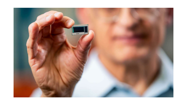
In September of this year, Intel announced that it was the first to launch a glass substrate for the next generation of advanced packaging, and plans to bring a complete solution to market in the next few years, so that the number of transistors in a single package continues to increase, continuing to push Moore's Law to meet the computing needs of data-centric applications.
While glass substrates are no stranger to the entire semiconductor industry, Intel has taken them to a new level with its vast manufacturing scale and outstanding technical talent. Recently, Intel's Assembly Test Technology Development explained why Intel is exploring glass substrates and how to make this technology a reality.
Computing power needs drive advanced packaging innovation
Advanced packaging is important for the development of Moore's Law. The need for more powerful and powerful processors has driven the creation of multi-chip integration technology, upgrading packaging from an essential step in the complete design of a processor to a key element.
The breakthrough in advanced packaging technology is reflected in multi-chip processor products, which integrate a series of chips designed to allow multiple chips to work together.
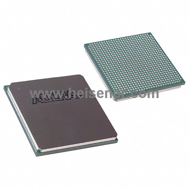
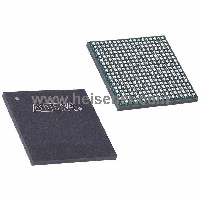
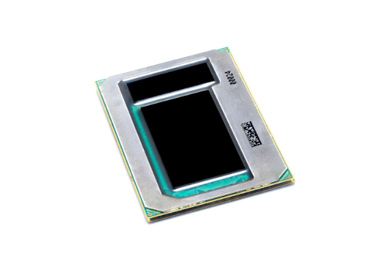
In the package, the main role of the substrate is to connect and protect the many chips inside. The substrate can be likened to a "spatial converter", in which nanoscale chips are connected to the substrate through micron-scale bond pads, which in turn convert these pads into millimeter-scale interconnects on the motherboard. To achieve this, the substrate needs to be flat and able to handle input currents and high-speed signals with high precision.
Comparative advantages of glass substrate
For more than 20 years, the main material used to build substrates has been organic plastic, but with the increasing number of chips and wires in a single package, organic substrates are approaching their physical limits.
Therefore, the idea of replacing organic substrates with glass substrates is widely recognized within the semiconductor industry. The glass substrate performs better in every way, being flatter (important for connecting flat silicon wafers to a very flat motherboard), stiffer (better able to hold more and more smaller lines), and more stable.
In addition to performing better in basic functions, the glass substrate is also expected to increase interconnection density and optical interconnection integration by a factor of 10, allowing future chips to process more data faster.
Addressing the technical challenges of glass substrates
Technology development is not easy, there are always many unknown difficulties, and the same is true of replacing organic substrates with glass substrates.
At the technical level, these challenges include: figuring out what kind of glass is more effective; How to layer metal and equipment to add microholes and wire; After the completion of the installation, how to better heat dissipation and withstand mechanical forces during the entire life cycle of the product.
In addition, there are many more practical problems: how to make the edge of the glass difficult to crack; How to partition the large glass substrate; How to protect the glass substrate from bouncing off or flying out of the conveyor belt or roller when transported in the factory.
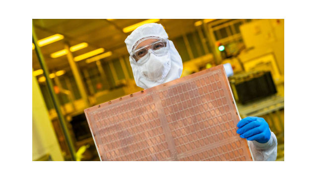
To meet these extraordinary challenges and implement glass substrate technology for next-generation advanced packaging, a dedicated team in Intel's Packaging Test Technology Development department has spent several years, conducting extensive debugging work, successfully solving many of the issues posed by the adoption of glass materials, and achieving the right combination of groundbreaking technologies and materials.
In the future, glass substrate technology will not only be used in Intel products, but will also be made available to external customers through Intel Foundry Service. As the packaging and Testing technology development department continues to refine its technology portfolio, Intel is planning its first in-house and contract products using glass substrates.
About US
Heisener Electronic is a famous international One Stop Purchasing Service Provider of Electronic Components. Based on the concept of Customer-orientation and Innovation, a good process control system, professional management team, advanced inventory management technology, we can provide one-stop electronic component supporting services that Heisener is the preferred partner for all the enterprises and research institutions.