The MPF102 is a general-purpose N-channel junction field-effect transistor (JFET), widely used in low-noise amplifiers, high input impedance circuits, and RF or audio signal processing applications. It features low leakage current, low noise, and high input impedance, making it ideal for use in preamplifier stages where signal amplification is required. With a typical TO-92 package, the MPF102 is well-suited for use as a switch or analog signal processing component in medium- to low-power electronic devices.
The operating principle of the MPF102 is based on the control of current through an electric field. In a JFET, current primarily flows between the drain and source terminals, while the gate voltage controls this current flow. For the MPF102, which is an N-channel device, applying a negative voltage to the gate relative to the source creates a depletion region within the semiconductor channel, restricting electron flow and thereby regulating the drain current (ID).
Under normal amplification operation, the MPF102 typically operates in a "self-bias" configuration, where a negative gate-to-source voltage is maintained, keeping the gate-source junction reverse-biased. As the gate voltage becomes more negative, the channel narrows, leading to a reduction in drain current. When the gate voltage drops below the cutoff voltage (V_GS(off)), the channel is completely pinched off, and the drain current becomes nearly zero.

Drain: The terminal where the current exits the device, typically connected to the load.
Source: The terminal where current enters the device, often tied to ground or a biasing network.
Gate: Controls the drain current by applying a negative bias to regulate channel conductivity.
| Parameter | Value |
| Device Type | N-channel JFET (Depletion Mode) |
| Package Type | TO-92-3 |
| Maximum Drain-Source Voltage (VDS) | 25V |
| Continuous Drain Current (ID) | 10mA |
| Maximum Power Dissipation (PD) | 350mW |
| Storage Temperature Range | -65°C to +150°C |
| Maximum Junction Temperature | +125°C |
| Gate-to-Source Voltage for Biasing (VGS) | -7.5V |
| Maximum Gate Current (IG) | 20mA |
| Input Capacitance (CGS) | 7pF |
| Reverse Transfer Capacitance (Crd) | 3pF |
General-purpose N-channel JFET
Depletion-mode operation
Low noise
High input impedance
Pb-free
RoHS standards
Low gate current
Analog and RF circuits
Low-Noise Amplifiers
High-Impedance Buffering
Pre-Amplification in Audio Systems
Signal Processing Circuits
Oscillators and Tuned Circuits
Voltage Control Circuit
Mixers and Modulators

The MPF102 N-channel JFET functions as a voltage-controlled resistor, amplifier, and electronic switch. Being an N-channel device, current conduction mainly involves electrons. It operates in depletion mode and is often used in common-source amplifier circuits.
Components:
MPF102 JFET, LED (load), -7.5V bias, 5V power supply
Connections:
- Drain → LED (load)
- Source → Ground
- Gate → Bias control
In default (gate at 0V), the JFET is ON, allowing current from drain to source, lighting the LED. When a -7.5V bias is applied to the gate, the JFET turns OFF, stops current flow and turns off the LED.
- At V<sub>GS</sub> = 0V: Low resistance, high current conduction
- At V<sub>GS</sub> = -7.5V: High resistance, minimal current (pinch-off condition)
In the pinch-off state, the MPF102 behaves like a voltage-controlled resistor, with V<sub>GS</sub> regulating the current flow.
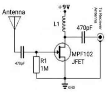
The MPF102 N-channel JFET can be used to design FM, AM, SW, MW, and HF antenna amplifier circuits for receiving weak signals and amplifying them with matched input and output impedance. The circuit is simple and can be built using just an MPF102, a couple of capacitors, an inductor, a resistor, and a 9V/12V power supply.
Due to its high input impedance and low noise characteristics, the MPF102 is ideal for active antenna preamplifiers, especially in applications like audio noise reduction, radio reception, and shortwave signal enhancement. A 470pF capacitor is used for noise filtering, and L1 acts as an RFC (Radio Frequency Choke) to amplify signals at specific frequency bands. The circuit operates without requiring any biasing current.
In case of noise or oscillation, adjusting L1 or checking the power supply and quiescent current (recommended 5–20mA) helps ensure stable operation.
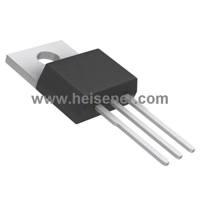
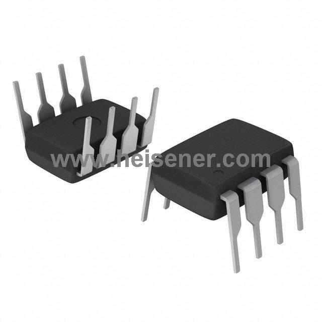
The MPF102 is housed in a TO-92-3 package, a compact and widely used through-hole plastic package with three leads—Drain, Source, and Gate. This package offers easy handling and good thermal performance.
The MPF102 JFET is manufactured by onsemi. onsemi is a globally leading semiconductor manufacturer headquartered in Arizona, USA, specializing in intelligent power and sensing solutions. Its products are widely used across automotive, industrial, communication, computing, and consumer electronics sectors, covering areas such as power management, analog devices, sensors, discrete components, and custom SoCs.
Datasheet PDF(https://dir.heisener.com/DatasheetDownload/MPF102_D74Z.pdf)
The MPF102 is a general-purpose N-channel JFET (Junction Field-Effect Transistor) that operates in depletion mode, commonly used for amplifying or switching low-level signals due to its high input impedance and low noise characteristics.
The MPF102 is used in RF amplifiers, audio preamplifiers, electronic switches, voltage-controlled resistors, and active antenna circuits for FM, AM, SW, MW, and HF signal amplification.
To connect the MPF102, ground the source terminal, apply the input signal or load to the drain, and use the gate terminal to control the bias voltage—typically with a negative voltage to adjust the drain current in amplification or switching applications.