STMicroelectronics' ST25R3916B-AQWT and ST25R3917B-AQWT NFC Forum reader chips offer high output power, high energy efficiency, and competitive prices. They support NFC initiator, target, read, and card emulation modes. Target applications include non- payments, device pairing, wireless charging, brand protection, and other industrial and consumer applications.
The new device introduces a more flexible Active Waveform Shaping (AWS) improvement that simplifies the RF output adjustment process and facilitates optimization of overshoot and undershoot issues. The RF adjustment operation is very easy, first modify the register settings on the supported GUI software, and then use the oscilloscope for quick verification. This technology simplifies EMVCo 3.1a and NFC Forum CR13 specification certification without having to deal with antenna matching issues.
The ST25R3916B and ST25R3917B provide up to 1.6W of RF output power and can drive antennas directly and efficiently. Dynamic Power Output (DPO) scaling technology allows designers to control radiated power within the upper and lower limits defined by the EMVCo and NFC Forum specifications.
ST25R3916B/17B integrates high noise immunity input structure and STMicroelectronics proprietary Noise Suppression Receiver (NSR), which has high anti-jamming capability to prevent nearby power supply, POS terminal and other equipment from interfering with the chip operation. Both devices also have strong immunity to radiated and conducted noise.
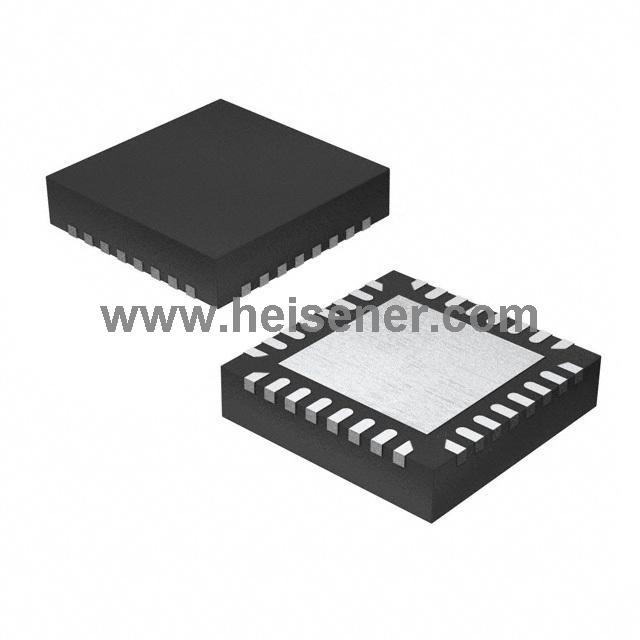
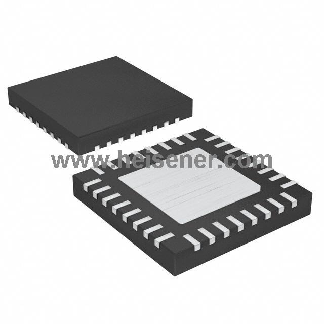
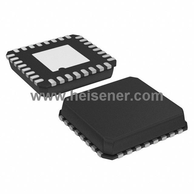
The supply voltage range of the ST25R3916B/17B chip is 2.4V to 5.5V, and the operating temperature range is -40°C to 105°C. The minimum operating voltage of the peripheral I/O circuit is 1.65V.The new products are available in a 32-pin VFQFPN 5mm x 5mm x 1mm package and a 36-bump wafer-level chip-level package (WLCSP).