A lot of different types of electronics use semiconductor devices, such as those that change power, communicate and process signals. Because stress (such as heat, high voltage, high current or change frequency) can hurt a device’s performance, dependability and efficiency, it is best to make semiconductor gadgets that are stress-resistant. The use of an asymmetrical structure, such as a three-phase current-source rectifier (CSR), is one way to reduce stress. When a structure is asymmetrical, it means that the device’s terminals or arms have different shapes or links.
A CSR is a type of power converter that changes alternating current to direct current with a step-down voltage function. It has six switches set up in three bridge arms. Each switch is made up of a transistor and a diode. You can make an asymmetrical structure by changing the inflow or outflow terminal of the CSR. This can lower the voltage and current load on the switches.
This article will talk about a new three-phase CSR with an asymmetrical structure and explore how it differs from a typical CSR, along with the pros and cons of the suggested CSR in terms of power loss, output filter, voltage stress and current stress.
Asymmetrical structure and modulation scheme
The suggested CSR has the same number of devices as a typical CSR, but the connection between the upper and lower arms is not symmetrical. The suggested CSR and a typical CSR are shown in Figure 1 in terms of their topological structure.
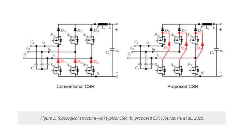
Figure 1 shows that the suggested CSR’s outflow terminal is not the same as its inflow terminal. Instead, the outflow terminal is connected between the diode and the transistor on the upper arms. In other words, the body diodes on the upper arms are added to the suggested CSR’s current path. The current path in the planned CSR has a small change with this new structure. An easy way to control CSRs is through space-vector pulse-width modulation (SVPWM), which is what the suggested CSR’s modulation scheme is based on. You can use two active vectors and one zero vector from a set of seven swapping states to make the input reference current space vector. This is what SVPWM is all about. The switching states are set by the different ways the switches in each arm can be turned on or off.
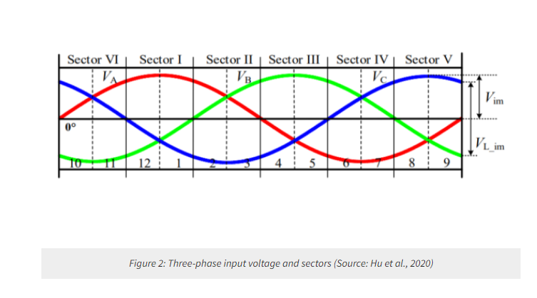
The input reference current space vector is made up of a current vector that rotates at a certain angle and has a certain amplitude. The modulation index and the sector angle are used to figure out the duty cycles for each vector. The SVPWM schematic diagram of the suggested CSR can be seen in Figure 2.
Stress characteristics and comparative analysis
One of the best things about using an uneven structure for the CSR is that it makes semiconductor devices less stressed. Stress is made up of voltage stress and current stress, which change based on how the CSR is working and what state it is in when it switches.
The voltage stress on a switch is the change in voltage between its two ends when it is not in use and current is flowing through its body diode. The voltage stress on a switch changes how well it blocks and how much it switches. The current that flows through a switch when it is on is called its current stress. This current also flows through the switch’s body diode. The current stress on a switch is determined by the current going through its body diode when it is turned on. This stress affects how well it handles heat and electrical loss. The amount of power that flows through a switch affects how well it handles heat and how much it loses.
There are two parts to a switch’s power loss: switching loss and transmission loss. The switching loss depends on how often the switches are made and how much power and current are stressed during the changes. There is a link between the conduction loss and the on-state resistance and current stress during conduction times.
The proposed CSR has a slightly higher switching loss than a typical CSR because it has an extra turn-on and turn-off in each switching period. However, it has a much lower conduction loss because half of the transistors are under less voltage and current stress. This means that the proposed CSR can work better than a typical CSR, especially when the modulation index is low and the freewheeling time is long.
One more good thing about the suggested CSR is that it can make the CSR system’s output filter smaller. The proposed CSR has a smaller output ripple voltage than a typical CSR because it has more than one freewheeling path. As a result, the suggested CSR can make the system more powerful and less expensive.
IDEAL’s SuperQ technology with asymmetrical structure
IDEAL Semiconductor’s SuperQ technology is an example of the asymmetrical CSR system discussed as a new approach to power device architecture. SuperQ, while primarily based on silicon, can also be adapted for use with alternative semiconductor materials like silicon carbide and gallium nitride. One distinguishing feature of SuperQ is its asymmetrical, charge-balanced structure, which facilitates increased doping levels, thinner epitaxial regions and larger conduction areas compared with conventional superjunction devices.
This unique structure translates into notable advantages, including reduced Rsp and lower switching losses, particularly in the 60-V to 850-V voltage range, when compared with currently available products. Additionally, SuperQ’s fabrication process follows a simplified CMOS-like flow suitable for 200-mm and 300-mm wafers, resulting in devices with the industry’s lowest resistances for selected packages.
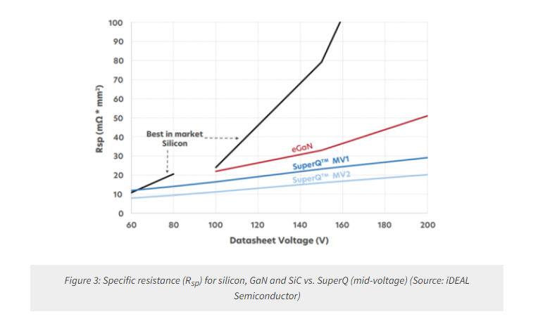
Examining SuperQ’s potential impact on the power industry, it is evident that this technology could bring substantial benefits. According to available information, SuperQ has the potential to achieve up to a 50% reduction in Rsp and a 70% decrease in switching losses compared with leading market alternatives. Such improvements could enhance the efficiency, reliability and thermal performance of power systems while also streamlining the manufacturing and packaging of power devices, potentially lowering costs.
Notably, SuperQ has progressed beyond the theoretical stage and has been successfully demonstrated across various test conditions and applications by iDEAL Semiconductor. This technology has showcased its prowess with examples like a 650-V/20-A device featuring an Rsp of just 6 mΩ in a TO-247 package and a 100-V/100-A device with an Rsp of only 0.8 mΩ in a D2PAK. Device featuring an RSP of just 6 mω in a to -247 package and a 100-v / 100-a device with an RSP of only 0.8 mω in a D2PAK package.
SuperQ stands out as a notable advancement in the power device sector, offering improved performance and potential cost savings while demonstrating adaptability to various semiconductor materials. These promising developments hint at its potential to reshape the industry and is in line with the novel three-phase CSR. While both SuperQ and the asymmetrical CSR hold significant promise, further independent evaluations and real-world applications are essential to gauge their full impact on the power device landscape.
About US
Heisener Electronic is a famous international One Stop Purchasing Service Provider of Electronic Components. Based on the concept of Customer-orientation and Innovation, a good process control system, professional management team, advanced inventory management technology, we can provide one-stop electronic component supporting services that Heisener is the preferred partner for all the enterprises and research institutions.