Due to their numerous applications and game-changing features, SiC MOSFETs have become extremely popular in the electronics market. WeEn Semiconductors has emerged as a leading developer and manufacturer of cutting-edge Silicon Carbide (SiC) Metal-Oxide-Semiconductor Field-Effect Transistors (MOSFETs), which represent a substantial improvement in power semiconductor technology.
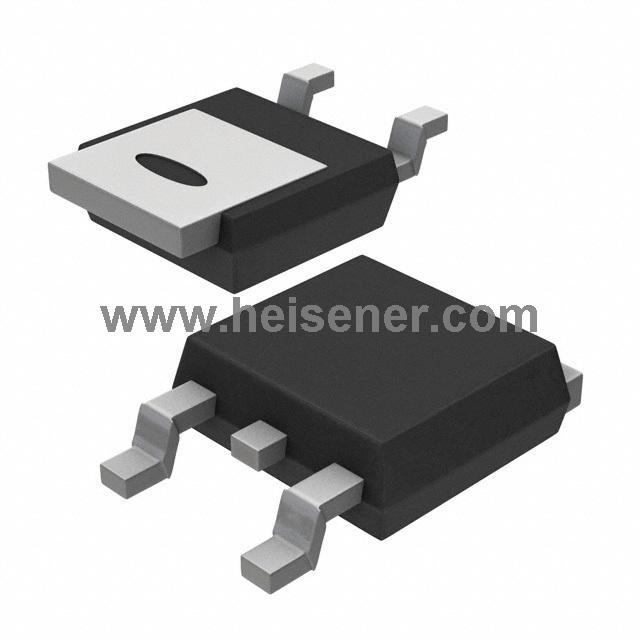
This article will focus on WeEn Semiconductor’s WNSC2M1K0170B7, an N-channel SiC MOSFET available in both TO263-7L and D2PACK-7L package versions.
Benefits of SiC MOSFETs
SiC MOSFETs’ fundamental benefit originates from the silicon carbide material itself. When compared to conventional silicon-based semiconductors, SiC stands out due to its exceptional physical and electrical features. Since silicon carbide has a larger bandgap than silicon, it can withstand higher temperatures and voltages. Because of this quality, both conduction and switching losses are minimized, leading to greater energy efficiency.
SiC’s strong thermal conductivity also aids in the reduction of heat, making it possible to create lightweight and space-saving power systems. In power electronics, where good heat management is vital for device reliability and durability, this quality is of paramount importance.
As a leading producer of SiC MOSFETs, WeEn Semiconductors is well-positioned to lead this technological shift. Their dedication to R&D, together with their emphasis on product quality and dependability, has established them as a go-to supplier in the semiconductor business.
WNSC2M1K0170B7: Technical Specifications
Silicon carbide (SiC) and other wide bandgap materials are preferable to silicon for several reasons. To begin, the bandgap of SiC is larger than that of silicon, with typical values of around 3.26 electron volts (eV) for SiC and 1.12 eV for silicon. SiC devices are well-suited for high-power and high-temperature applications due to their increased bandgap, which allows them to operate at higher temperatures without experiencing damage or breakdown. As indicated in the datasheet, the WNSC2M1K0170B7 SiC MOSFET offers a junction temperature (TJ) range of -55°C to +175°C. This value is higher than that of silicon-based MOSFET transistors, which typically have a TJ(max) of 150°C.
Secondly, the critical parameter of electron mobility in SiC is significantly higher than that in silicon. The higher electron mobility enhances the speed at which charge carriers can move through the material, contributing to faster switching speeds in electronic devices. This property is particularly advantageous in power electronics applications where efficiency is paramount, as it reduces both conduction and switching losses. The velocities of electrons (N-channel MOSFET) and holes (P-channel MOSFET) can be accelerated by an electric field, and this acceleration is quantified by their respective mobilities (μ). The mobility (μ) is defined as the ratio of the velocity to the electric field (E). Increased mobility (μ) corresponds to enhanced electrical conductivity, leading to reduced resistance. The term used to describe the highest achievable velocity is referred to as the saturation drift velocity.
A SiC MOSFET like the WeEn WNSC2M1K0170B7 features a saturation drift velocity of 2.7 · 107 cm/s, which is much higher compared to silicon (~ 1.0 · 107 cm/s). This characteristic allows the device to operate at high switching frequencies without causing switching losses and heat generation issues.
Electron mobility is a measure of how quickly electrons can move through a material in response to an electric field. Since SiC has higher electron mobility than Silicon, this means that electrons can traverse the channel more rapidly, leading to a lower on-resistance (RDS(on)). Additionally, the wider bandgap of SiC contributes to a thinner depletion region in the channel, allowing for lower on-resistance as electrons can move more easily between the source and the drain terminals.
The WNSC2M1K0170B7 features a drain-source on-resistance, in static conditions (VGS = 15 V; ID = 1 A; TJ = 25°C), of 1,000 mΩ. The drain-source on-resistance is often expressed relative to the channel width (W) and is normalized per unit width. The equation for normalized drain-source on-resistance is given by:
Where:
RDS(on) is the normalized drain-source on-resistance
RDS is the actual drain-source on-resistance
W is the channel width of the MOSFET.
In MOSFETs, the on-resistance is a critical parameter as it directly affects the power dissipation and efficiency of the device. Lower on-resistance leads to better conduction and reduced power losses. Engineers often strive to minimize RDS(on) to improve the performance of MOSFETs in various electronic applications, such as power amplifiers, voltage regulators, and switching power supplies.
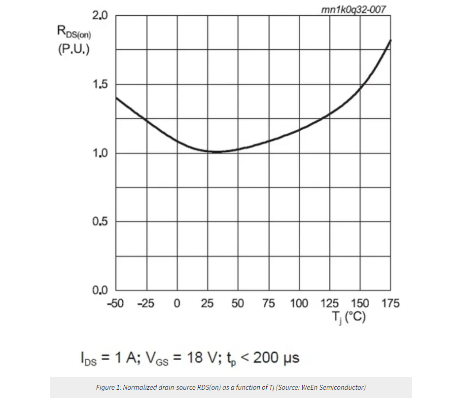
The WNSC2M1K0170B7’s normalized drain-source on-state resistance as a function of junction temperature is shown in Figure 1. The graph has been traced under the following operating conditions: IDS = 1 A; VGS = 18 V; tp < 200 μs.
Furthermore, SiC exhibits superior thermal conductivity compared to silicon. The thermal conductivity of SiC is approximately three times higher than that of silicon. This elevated thermal conductivity facilitates better heat dissipation, enabling SiC devices to operate at higher power levels and in more demanding thermal environments. Improved thermal performance is crucial for the reliability and longevity of electronic components.
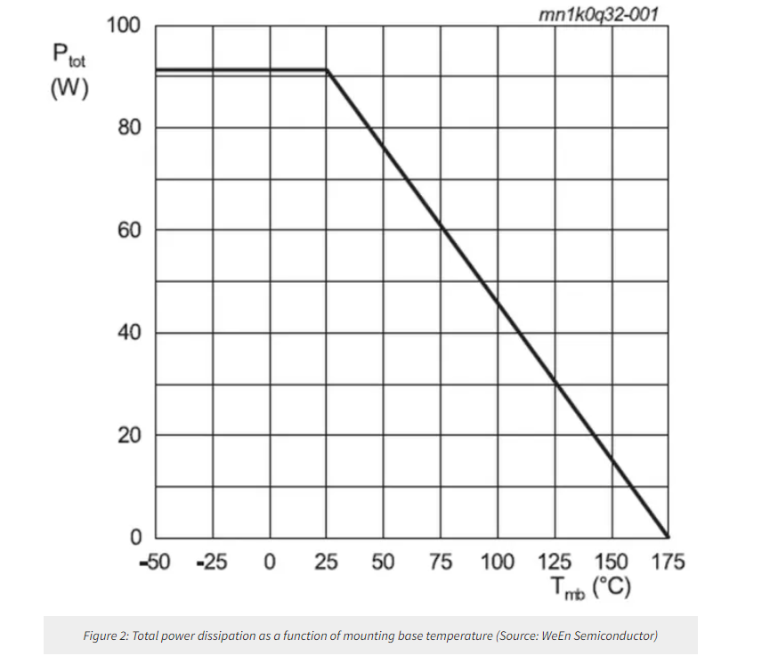
The WNSC2M1K0170B7 has a total power dissipation of 91W and a thermal resistance from the junction to the mounting base of 1.64K /W. As shown in Figure 2, referred to the WNSC2M1K0170B7 MOSFET in the TO263-7L package, As shown in Figure 2, referred to the WNSC2M1K0170B7 MOSFET in the TO263-7L package, the power dissipation varies with different temperatures. An excellent thermal conductivity allows designers to reduce or eliminate the need for external cooling systems.
The higher breakdown electric field strength of SiC devices, often exceeding 10 times that of silicon, allows them to operate at higher voltages, making them suitable for applications requiring elevated voltage and power levels. The WNSC2M1K0170B7 SiC MOSFET achieves a drain-source breakdown voltage of 1,700V; this increased voltage capability is advantageous in power distribution systems and high-voltage power electronics.
Moreover, the device simplifies the design of the gate drive because of:
● A wide range of the gate-source (VGS) voltage, from -5V up to +18V (maximum range is from -10V to +22V)
● The device can be turned off by applying a 0V gate voltage
● The gate-source threshold voltage (VTH) has a typical value of 3.2V@25°C and 2.4V@150°C (ID = 0.8 mA, and VDS = 10 V)
Other relevant characteristics of the WNSC2M1K0170B7 include a fast switching time, low turn-on and turn-off energies, and the ability to be connected in parallel, thus helping to achieve higher currents and improving thermal management.
Applications of the WNSC2M1K0170B7
SiC MOSFETs find applications across various industries, prominently in power electronics and electric power systems. One of the primary use cases is in power converters and inverters, where SiC devices enable higher power density and efficiency. Electric vehicles (EVs) and renewable energy systems benefit significantly from SiC MOSFETs, as they allow for compact and lightweight power electronic systems, thereby extending the driving range of EVs and enhancing the efficiency of solar inverters and wind converters.
Moreover, the high-speed switching capability of SiC MOSFETs makes them suitable for applications requiring fast switching frequencies. This is advantageous in power supplies, where higher switching frequencies result in smaller passive components, reduced system size, and improved transient response.
In the realm of motor drives and traction inverters for electric vehicles, SiC MOSFETs contribute to increased efficiency and power density. The ability to operate at higher temperatures enables these devices to thrive in demanding automotive environments, ensuring reliable and robust performance.
The high efficiency and ability to operate at high voltages open the door to EV chargers, UPS, solar string inverters, and solar optimizer applications.
Conclusion
Silicon Carbide MOSFETs, particularly those manufactured by WeEn Semiconductors, represent a paradigm shift in power semiconductor technology. The advantages of SiC, including high-temperature operation, reduced losses, and increased efficiency, have paved the way for transformative applications in electric vehicles, renewable energy systems, and power electronics. As the industry continues to embrace SiC technology, the collaboration between manufacturers like WeEn and the broader electronics ecosystem is crucial for driving innovation and shaping the future of power electronics.
About US
Heisener Electronic is a famous international One Stop Purchasing Service Provider of Electronic Components. Based on the concept of Customer-orientation and Innovation, a good process control system, professional management team, advanced inventory management technology, we can provide one-stop electronic component supporting services that Heisener is the preferred partner for all the enterprises and research institutions.