Silicon carbide (SiC) power devices have been widely used in server power supplies, energy storage systems and photovoltaic inverters. In recent years, the shift to electric drive in the automotive industry has driven the growth of silicon carbide (SiC) applications, and has led design engineers to focus more on the benefits of the technology and broaden its application areas.
Selective device technique
Regardless of the application field, every power supply design begins by answering some of the same basic questions: What is the input voltage, output voltage, and output current? Next, designers consider the performance criteria they are trying to achieve in the final product. Currently, power designers can utilize a variety of devices to meet these standards, including gallium nitride (GaN), silicon carbide (SiC), and various silicon-based (Si) technologies such as MOSFETs, insulated gate bipolar transistors (IGBTs), and super junction (SJ) devices (Figure 1).
Figure 1: Each of these technologies has its own advantages and most applicable application areas

When the rated breakdown voltage is below 400 V and the design requires relatively low frequency operation at less than 1 kW, silicon (Si) is usually a good choice. Gallium nitride (GaN) is an excellent choice when manufacturing compact applications such as USB chargers that require high switching frequencies to reduce the size of magnetic components. Igbts can be considered for use with silicon carbide (SiC) when the power exceeds 1 kW and the rated voltage is between 600 V and 1,700 V at low frequencies. However, for higher switching frequencies or higher power densities, silicon carbide (SiC) is the best choice.
Center of choice
In Figure 1, the central position formed between multiple choices is at moderately high voltages and switching frequencies. However, the high efficiency of silicon carbide (SiC) makes it a compelling choice, as the trade-off between bill of material costs and operating costs can be a deciding factor.
Wolfspeed Silicon Carbide (SiC) devices have extremely low on-resistance, which means low on-loss and high efficiency. In this regard, silicon carbide (SiC) outperforms other technologies in all applications compared to silicon (Si) and gallium nitride (GaN) (Figure 2). The properties of the material make the on-resistance fluctuate little with temperature, while the RDS(ON) of gallium nitride (GaN) and silicon (Si) increase by 2.5 times or more than the rated value at room temperature.
Figure 2: Wolfspeed Silicon Carbide (SiC) devices maintain stable low RDS(ON) over a wide temperature range

Realize the transformation of PFC technology
Modern power supply rectifiers have evolved from simple bridge rectifiers that require only a "large farad capacitor" to smooth the DC output. The added passive power factor correction (PFC) phase usually comes with an power frequency LC filter. This method is suitable for relatively low-power applications where efficiency and size are not strictly required (Figure 3).
Figure 3: Full-bridge rectifiers evolve from simple PFC-free to basic bridgeless PFCS
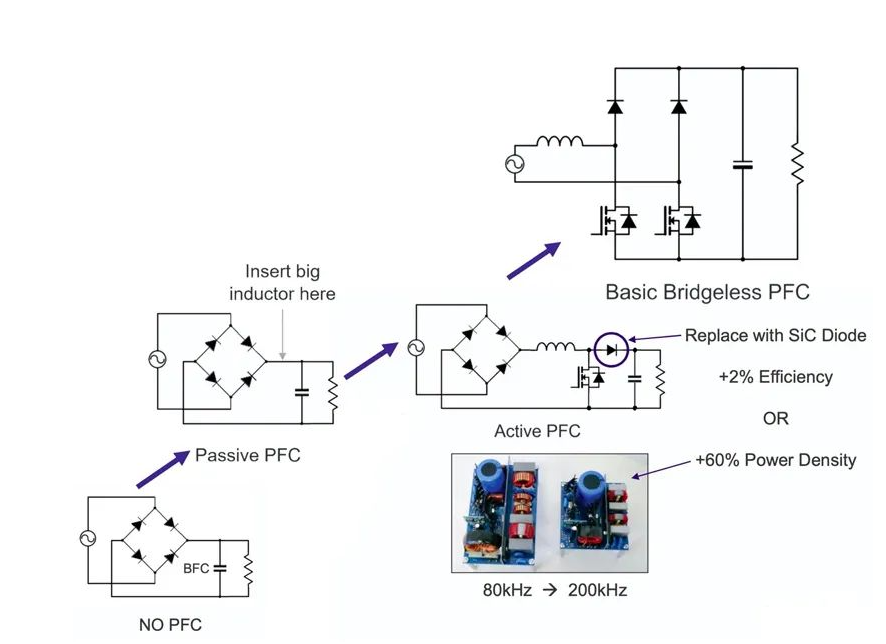
Today, in most switching power supplies, the boost converter is used as an active PFC after the diode rectifier bridge, and its switching frequency is several orders of magnitude higher than the power frequency, so smaller inductors and capacitors can be used. Depending on the application, replacing silicon (Si) -based diodes with silicon carbide (SiC) diodes in active PFC circuits can improve energy efficiency by two to three percentage points.
On the other hand, increasing the switching frequency from 80 kHz to 200 kHz can reduce the form factor or increase the power density by up to 60%. In general, increasing the switching frequency helps to reduce the size of the inductor and reduce the copper loss of the inductor.
However, when the frequency is increased from 200 kHz to 400 kHz, the copper loss levels off, while the inductor core loss continues to increase. The result is diminishing returns, a 10 to 15 percent reduction in size and a 10 to 15 percent increase in power loss. For applications where downsizing is necessary, this may be an acceptable compromise.
To increase the efficiency level above 90%, the circuit must be redrawn to remove the diode bridge. To remove the diode, one way is to move the inductor to the AC input and replace the two bottom diodes in the bridge circuit with two MOSFETs. The switch on the left raises the voltage in the positive half cycle, and the switch on the right raises the voltage in the negative half cycle.
The challenge with basic bridged circuits is that the high frequency switching nodes are directly connected to the AC input, and the DC ground is floating relative to the AC input. This causes any parasitic capacitance to become directly common-mode EMI. A common way to solve this problem is by using a bridge-free dual Boost, or semi-bridge-free (Figure 4, left).
Figure 4: Comparison of the bridge-free dual Boost solution (left) and the totem pole topology (right) with a full-bridge evolution using silicon carbide (SiC)
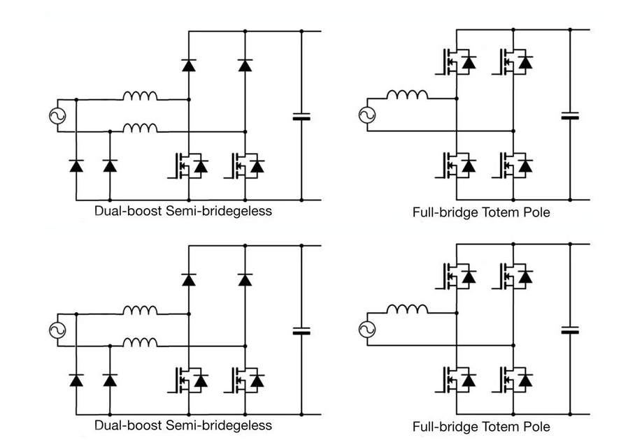
In this topology, the two diodes at the bottom left eliminate the floating ground problem, while the split inductor eliminates the direct connection of the switching node to the AC power supply, thus solving the common mode EMI problem. While silicon (Si) MOSFETs can be used, they have a maximum efficiency of 95 to 96 percent and a larger footprint, requiring two inductors, which can lead to a higher total bill of material cost.
Totem pole topology
The Totem pole topology is an alternative to the bridge-free dual Boost topology, which takes its name from the way transistors are stacked on top of each other (Figure 4, right). As shown in the figure, the totem pole can be made into a full-bridge MOSFET version, or it can be made into a no-bridge version, that is, the MOSFET on the right low-frequency bridge arm is replaced with a diode.
If operating in continuous on-mode (CCM) conditions, the biggest challenge facing totem pole topology is the reverse recovery charge from MOSFET body diodes. In the process of switching from the low-voltage side switch to the high-voltage side switch, the two MOSFETs cannot be switched on at the same time, and the body diodemust be switched on within the dead time. The reverse recovery properties of silicon (Si) reduce its efficiency (Figure 5).
In this topology, the two diodes at the bottom left eliminate the floating ground problem, while the split inductor eliminates the direct connection of the switching node to the AC power supply, thus solving the common mode EMI problem. While silicon (Si) MOSFETs can be used, they have a maximum efficiency of 95 to 96 percent and a larger footprint, requiring two inductors, which can lead to a higher total bill of material cost.
Totem pole topology
The Totem pole topology is an alternative to the bridge-free dual Boost topology, which takes its name from the way transistors are stacked on top of each other (Figure 4, right). As shown in the figure, the totem pole can be made into a full-bridge MOSFET version, or it can be made into a no-bridge version, that is, the MOSFET on the right low-frequency bridge arm is replaced with a diode.
If operating in continuous on-mode (CCM) conditions, the biggest challenge facing totem pole topology is the reverse recovery charge from MOSFET body diodes. In the process of switching from the low-voltage side switch to the high-voltage side switch, the two MOSFETs cannot be switched on at the same time, and the body diode must be switched on within the dead time. The reverse recovery properties of silicon (Si) reduce its efficiency (Figure 5).
Figure 5: Reverse recovery comparison of silicon carbide (SiC) and silicon (Si) body diodes
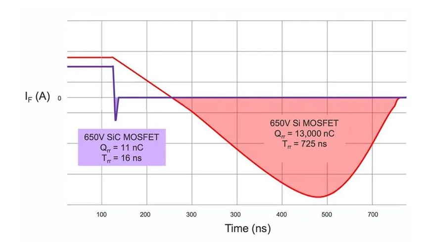
In all hard switching power supply designs, reverse recovery loss occurs when the body diode must be switched on. Silicon carbide (SiC) has no minority carriers, so the reverse recovery current is almost zero.
The loss of silicon (Si) MOSFETs is several orders of magnitude higher. This is why silicon (Si) devices cannot be used in totem poles.
Full bridge totem pole or mixed totem pole?
Totem poles with synchronous rectification are the most efficient way to implement them. While it can use silicon (Si) MOSFETs in low-frequency bridge arms, only all four silicon carbide (SiC) MOSFETs achieve bidirectional operation - for example, in applications that connect to smart grids, there are some trade-offs in complexity and bill of material costs.
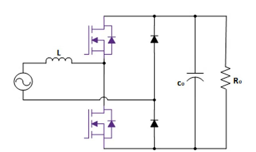
Most cost-sensitive applications, including server power, employ bridge-less or "hybrid" totem pole topologies, using inexpensive PIN diodes on low-frequency bridge arms (Figure 6). It has the advantage of the minimal number of components used, and with the introduction of Wolfspeed's 650V withstand voltage class C3M Silicon Carbide (SiC) MOSFETs, it is a cost-effective way to implement, reducing light load efficiency by less than 0.5% compared to full Bridges.
Figure 6: A "hybrid" totem pole topology using silicon carbide (SiC) MOSFETs and diodes
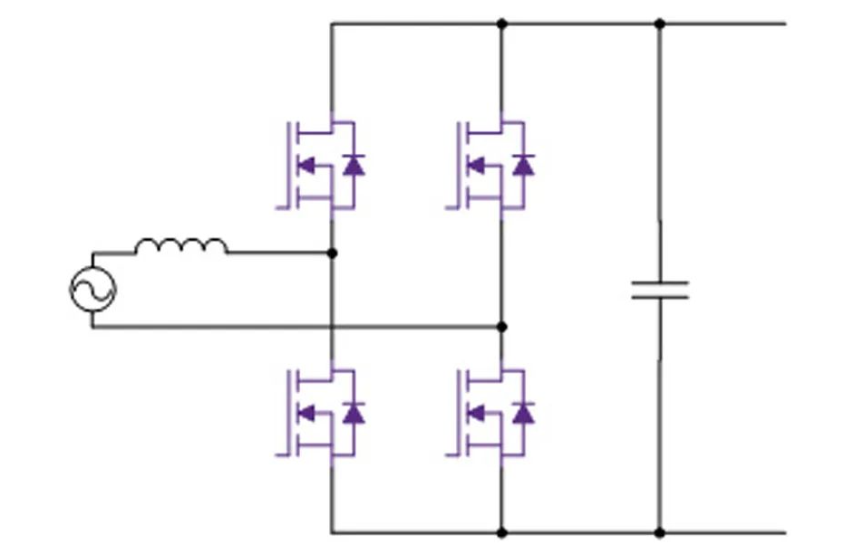
However, as shown in Figure 7, to realize the full potential of the totem pole PFC topology and achieve peak efficiency above 99%, a full-bridge totem pole PFC utilizing all four silicon carbide (SiC) MOSFETs can eliminate the diode voltage drop, resulting in the highest efficiency and power density.
Figure 7: Full-bridge totem pole PFC with all-silicon carbide (SiC) MOSFETs
About US
Heisener Electronic is a famous international One Stop Purchasing Service Provider of Electronic Components. Based on the concept of Customer-orientation and Innovation, a good process control system, professional management team, advanced inventory management technology, we can provide one-stop electronic component supporting services that Heisener is the preferred partner for all the enterprises and research institutions.